Portfolio / Selected Work
Three systems.
One process-driven way
of engineering.
Selected projects across polymer MEMS, microfabrication and microfluidic systems—connecting physical principles with fabrication, experimental validation and repeatable performance.
Case Studies
03 selected
Period
2019–2026
Focus
MEMS & microfabrication
01 — Selected Work
Choose a project
to explore.
Hover or select to preview
Integrated Colloidal Scanning Probe Platform
Polymer MEMS · Process Integration
Particle placement integrated into a unified fabrication architecture
Low-Power SU-8 Thermal Actuator
Multiphysics · Polymer Microfabrication
63 µm measured motion from a model-to-hardware workflow
Cavitation-on-Chip Microfluidic Reactor
Microfluidics · High-Speed Imaging
2.24 MPa inception pressure—approximately 46% lower
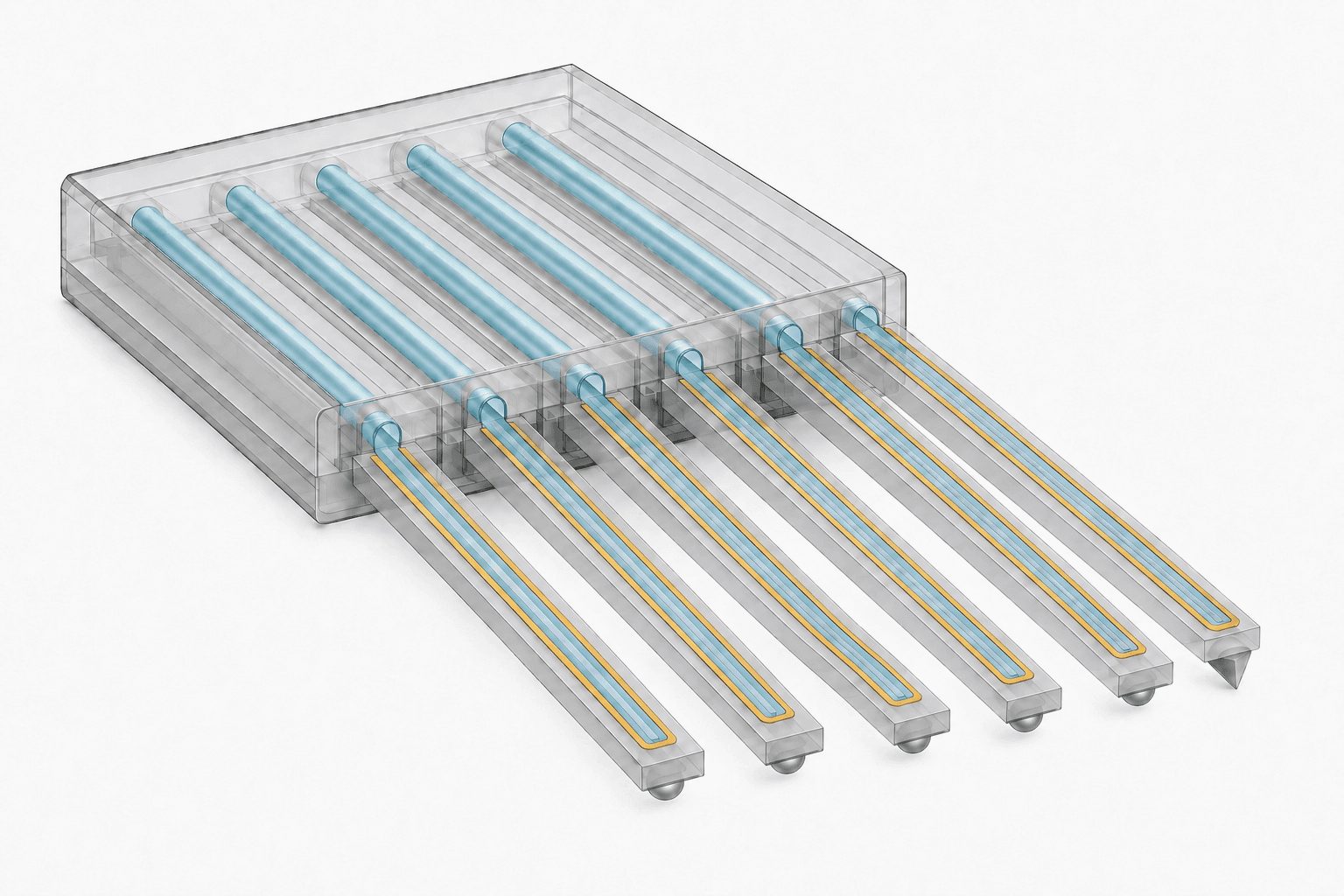
Project 01 / Process Integration
Integrated Colloidal
Scanning Probe Platform
Turning particle placement from a manual assembly step into part of a unified microfabrication process.
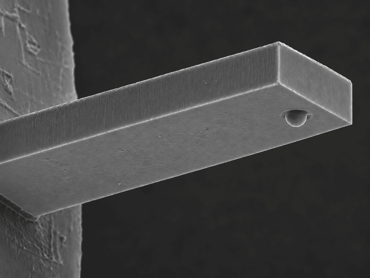
Challenge
Conventional colloidal probes depend on slow, probe-by-probe pick-and-place assembly.
Engineering Response
A common platform connecting custom tip geometry, particle placement, fiber alignment and optical actuation.
My Role
Design · Microfabrication · Process integration · Characterization
System
Unified probe architecture
Feature Scale
5–30 µm
Tip Platform
Multiple geometries
Integration
Particle + fiber + optical actuation
Project 02 / Model to Hardware
Low-Power SU-8
Thermal Actuator
A coupled electrical–thermal–structural model guided geometry and process decisions before a two-mask SU-8/Cu device was fabricated and measured.
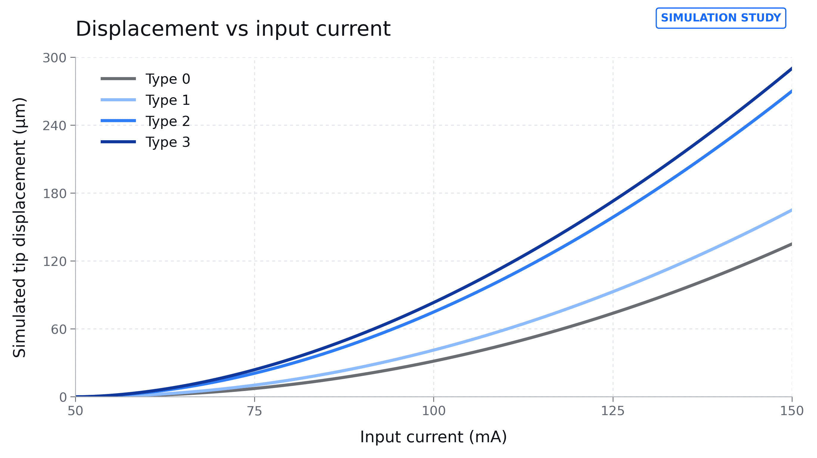
Model the motion.
Couple electrical input, Joule heating, thermal expansion and structural deformation.
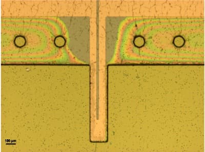
Build with two masks.
Translate the selected geometry into aligned metal and polymer layers.
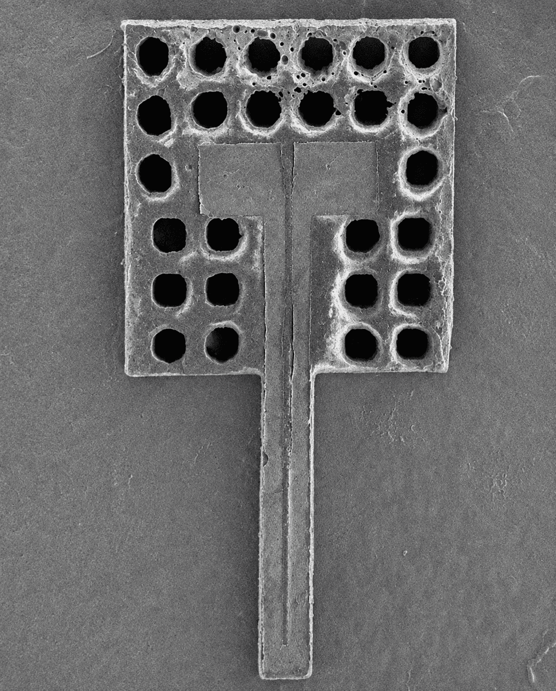
Validate the hardware.
Measure the out-of-plane response and compare the real device with the predicted behavior.
Measured Motion
63 µm
Input Power
36 mW
Simulated Response
≈200 ms
Engineering Scope
Modelling · Fabrication · Experimental validation
Project 03 / High-Speed Flow Characterization
Cavitation-on-Chip
Microfluidic Reactor
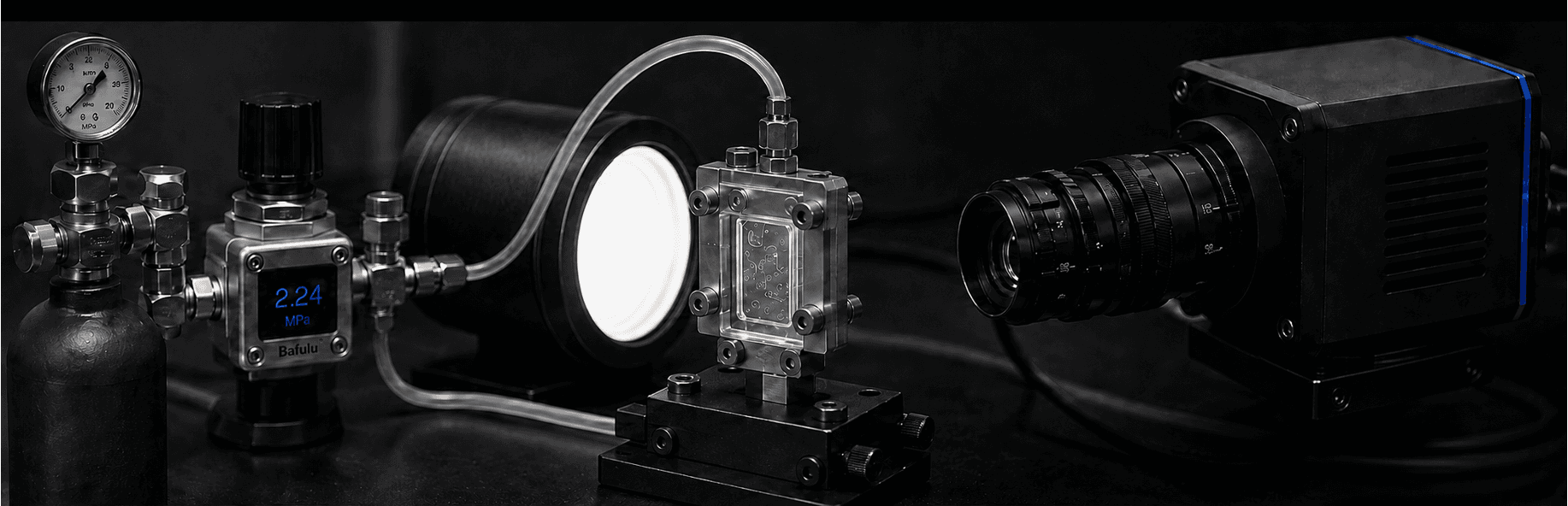
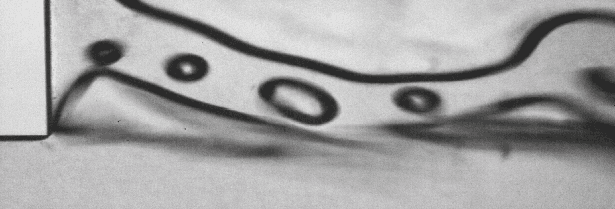
An eight-orifice silicon–glass reactor engineered to trigger cavitation at lower pressure while producing several useful flow regimes on one chip.
Pressure-driven test rig · Backlit high-speed imaging
The Shift
Lower pressure.
More useful flow states.
My Contribution
Device co-development · Experimental testing
High-speed imaging · Flow-regime analysis
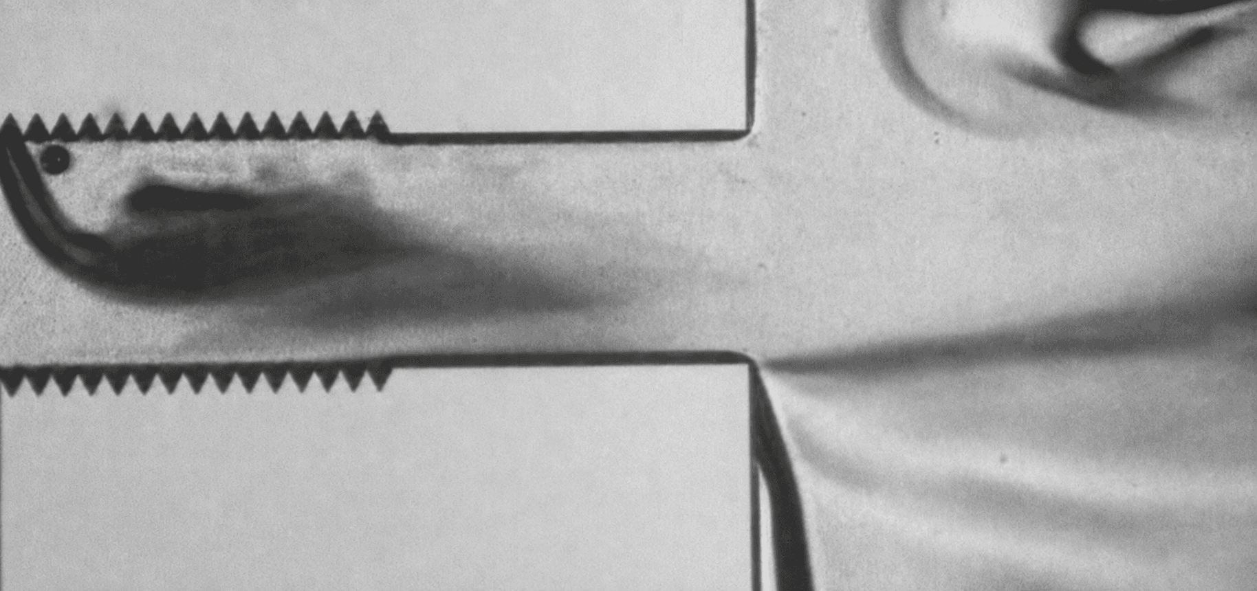
01Sheet Cavity
02Fully Developed Oscillating Flow
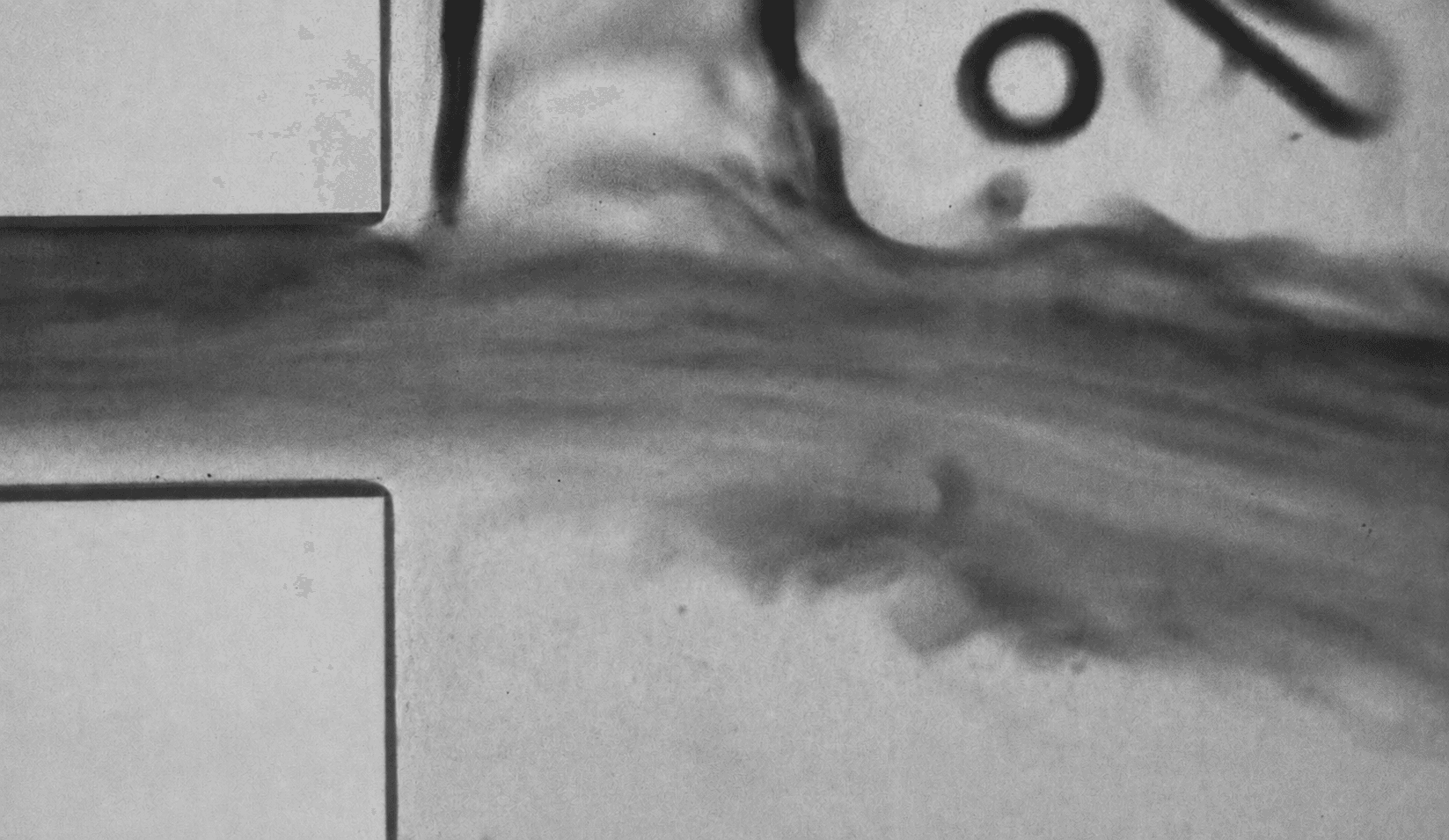
03Downstream Bubble Morphology
Parallel Architecture
8 micro-orifices
Cavitation Inception
2.24 MPa
vs. Reference Geometry
≈46% lower
High-Speed Capture
7,000 fps
Across the Work / Engineering Practice
Three projects.
One engineering practice.
Across microprobes, thermal actuation and two-phase flow, the work follows the same discipline: frame the physics, make the architecture manufacturable, and let evidence drive the next decision.
01 / Microprobes
Integrated Colloidal Scanning Probe Platform
Architecture
SU-8 probe · Colloidal tips · Aligned optical fibers
Engineering Move
Replace serial assembly with a process-integrated platform
Primary Evidence
SEM inspection · Optical function validation
Outcome
Alignment preserved through release
02 / Microactuators
Low-Power SU-8 Thermal Actuator
Architecture
SU-8/Cu bimorph actuator · Two-mask device process
Engineering Move
Couple electrical, thermal and structural prediction
Primary Evidence
Simulation · Measured out-of-plane motion
Outcome
63 µm motion · 36 mW
03 / Microfluidics
Cavitation-on-Chip Microfluidic Reactor
Architecture
Eight parallel roughened micro-orifices · Silicon-glass
Engineering Move
Trigger cavitation earlier while unlocking multiple flow states
Primary Evidence
7,000 fps imaging · Flow-regime analysis across eight channels
Outcome
2.24 MPa · ≈46% lower
Working Range
Microfabrication · Coupled physics · Experimental systems · Evidence-led iteration
Start a Conversation
Let’s turn difficult physical problems into manufacturable devices.
Open to R&D roles and collaborations across MEMS, microfabrication, semiconductor process development, microfluidics and experimental systems.
ali.hp.shafaghi@gmail.com
Based In
Munich, Germany
Work Authorization
Unrestricted · Germany
Connect
LinkedInDocument
Download résuméAli Shafaghi
MEMS & Microfabrication Engineer