Diagnosing MEMS Fabrication Failures: From Defect Signature to Root Cause
A disciplined method for turning visible defects into testable mechanisms, discriminating evidence and corrective actions.
A MEMS defect is often most visible at the end of a process and most understandable several steps earlier.
A film may delaminate during release even though its interface was weakened during surface preparation. A suspended beam may appear stuck after drying, but incomplete sacrificial-layer removal, a particle or residual stress may be responsible. An etch may stop early in dense features while open areas reach the target depth, although both received the same recipe.
“Delamination,” “stiction,” “under-etch” and “misalignment” describe observations. They do not yet identify the mechanism, the step where it originated or the evidence needed to prevent recurrence.
Effective failure analysis follows a disciplined sequence:
Defect signature -> competing mechanisms -> discriminating evidence -> corrective action -> recurrence check
Engineering principle
The location where a defect becomes visible is not necessarily the location where it originated.
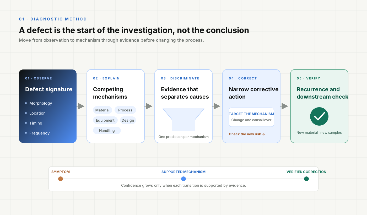
Failure analysis is not process optimization
Process development asks: Which operating region produces acceptable outputs despite expected variation? Failure analysis asks: Which mechanism best explains this particular pattern of evidence?
The disciplines share metrology, experiments and physical reasoning, but their logic differs. Development maps a response across a process window. Diagnosis narrows plausible causes until one explanation accounts for the signature better than its alternatives. Its purpose is not to tune a recipe. It is to decide what should be tuned, and why.
1. Preserve and describe the evidence
The first response to a failed wafer should usually be observation, not reprocessing. Cleaning can remove residue; another drying cycle can move a released structure; cleaving can introduce fractures; electron-beam charging can disturb an isolated feature.
Before an irreversible step, record the wafer, die and feature identity; the last confirmed-good inspection; when the defect was first observed; relevant delays; tool and material history; and every intervention after detection. Preserve an untouched reference when possible. Use separate samples for non-destructive inspection, cross-sectioning and confirmation experiments.
A useful failure signature is specific enough that another engineer could identify the same population without hearing the proposed cause. “Poor adhesion” is an interpretation. “Film lifting begins at patterned corners after the release bath and affects 18 of 24 edge dies” is an observation.
Describe the signature along six dimensions:
| Dimension | What to record |
|---|---|
| Morphology | Crack, blister, wrinkle, residue, notch, collapse, particle or missing feature |
| Location | Edge or center, dense or isolated pattern, corner or flat interface, one layer or several |
| Direction | Relation to crystal orientation, spin, flow, scan or alignment axis |
| Timing | Present immediately, revealed later, or produced after storage or testing |
| Frequency | One feature, die, radial zone, wafer, lot or every run |
| Correlation | Geometry, thickness, tool position, material lot, operator or elapsed time |
Spatial patterns are powerful discriminators. A radial distribution suggests different mechanisms from a pattern that follows local feature density. Corner initiation can point toward stress concentration, coverage or development. A failure above a critical beam length may implicate restoring stiffness, transport distance or accumulated stress.
Decision rule
Do not perform a destructive inspection until you can state which hypothesis it will test and what result would strengthen or weaken that hypothesis.
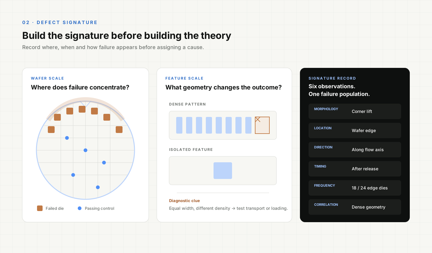
2. Reconstruct the timeline and build competing mechanisms
The step after which a defect becomes visible gives an upper bound on its origin, not a final answer.
Identify the last point where the relevant feature or interface was known to be acceptable. Then list every later thermal, chemical, plasma, mechanical and environmental exposure, including waiting periods. For each step ask:
- Could it create the observed morphology?
- Could it produce the spatial and geometric distribution?
- Could the defect remain hidden until it was detected?
Release, for example, removes mechanical support and exposes stored stress. A film may look intact throughout deposition and patterning, then curl, crack or delaminate when the sacrificial layer disappears. Packaging can similarly expose latent weaknesses through heat, pressure, outgassing, die handling or particles. Sandia’s packaging work shows that package materials and package-induced stress can affect MEMS performance rather than merely protect the die.1
Build a short set of mechanisms across five families:
- Material and interface: contamination, surface chemistry, adhesion, residual stress, thermal mismatch or trapped solvent.
- Process: exposure, bake history, deposition state, etch transport, selectivity, rinse or drying.
- Equipment: chamber condition, temperature, flow, focus, contact, calibration or clamping.
- Design: pattern density, aspect ratio, unsupported span, corners or topography.
- Handling and environment: particles, mechanical contact, humidity, storage, charging or packaging.
Rank each hypothesis by physical plausibility, fit to the complete signature, consistency with the timeline and testability. A strong hypothesis makes a distinct prediction. If two explanations predict the same result in the proposed experiment, that experiment will not separate them.
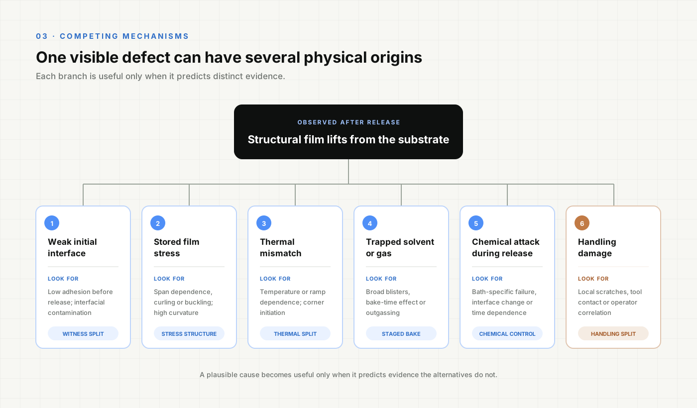
3. Choose tests that separate the mechanisms
The best next test is the one most likely to change the hypothesis ranking—not the most sophisticated instrument available.
Begin with low-risk evidence: process records, wafer maps, known-good controls, optical inspection, dimensional metrology, film-thickness maps, profilometry and electrical continuity. Move to SEM, material analysis, focused-ion-beam cross-sections or destructive adhesion testing when each answers a defined unresolved question.
Higher resolution is not automatically higher diagnostic value. An SEM can describe a fracture surface without revealing whether residual stress, chemical weakening or handling initiated the failure. A simple split in which identical witness films receive or avoid one chemical exposure may separate those mechanisms more decisively.
Dedicated test structures can isolate properties that a completed device mixes together. NIST’s MEMS 5-in-1 reference material, for example, includes structures for residual strain, strain gradient, Young’s modulus, step height and in-plane length.2
Use evidence in this order:
- Define the affected population.
- Localize where failure initiates.
- Identify the changed material or structural condition.
- Reproduce or suppress the proposed mechanism.
- Verify that the correction prevents recurrence.
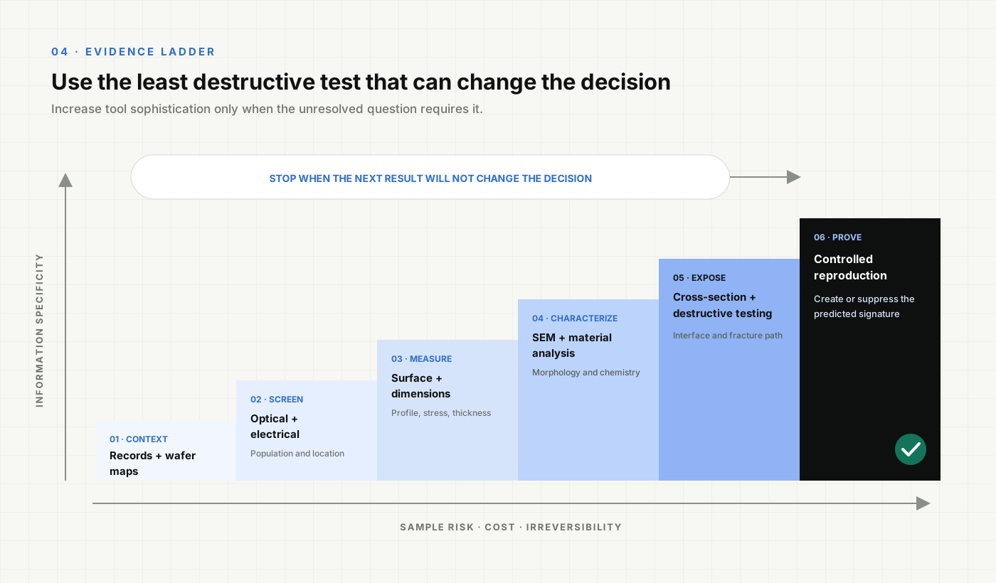
A practical diagnostic matrix
This matrix is not a catalogue of fixed causes. It shows the reasoning pattern: preserve competing mechanisms, select discriminating evidence and anticipate the risk introduced by a correction.
| Failure signature | Competing mechanisms | Confirmation method | Corrective direction | New risk |
|---|---|---|---|---|
| Resist lifts during develop or etch | Moisture, contamination, surface chemistry, aggressive exposure | Surface/contact-angle check; cleaned witness split; wafer map | Improve dehydration or surface preparation; reduce exposure | CD shift, residue, altered stripping or downstream adhesion |
| Film blisters, cracks or delaminates | Weak interface, stress or stress gradient, trapped species, thermal mismatch | Stress structures or wafer curvature; cross-section; thermal/chemical split | Modify interface, deposition state or thermal sequence | Changed resistivity, step coverage, etch or release behavior |
| Etch depth follows layout | Loading, aspect-ratio transport, mask erosion, thermal non-uniformity | Map depth by width, density and position; measure remaining mask | Adjust layout loading, cycle balance, transport or endpoint | Roughness, selectivity loss, notching or lower throughput |
| Polymer cracks at corners | Thermal gradient, solvent loss, over-crosslinking, topographic stress concentration | Bake split; staged inspection; thickness and corner correlation | Slow ramps; adjust bake/exposure; redesign corner | Longer cycle, incomplete crosslinking, swelling or hard removal |
| Released structures collapse | Capillary stiction, incomplete release, residue, particles, stress, charging | Compare pre/post-dry state and drying routes; residue or deflection map | Change rinse/dry or release completeness; control surface/charge | Altered surface chemistry, dynamics, compatibility or complexity |
| Overlay changes across wafer | Mark quality, distortion, topography, focus/contact or stage error | Overlay-vernier map; mark image review; orientation/tool split | Improve marks; correct systematic offset or distortion | Lost area, added steps or mark damage |
| Failure begins after packaging | Particles, contact, bond wire, die-attach stress, outgassing or humidity | Compare pre/post-package function; inspect package; controlled handling split | Change handling, cleaning, material or assembly sequence | Added handling, altered damping, hermeticity or thermal path |
Three diagnostic walkthroughs
Delamination after release
A film that lifts during wet release may have a weak initial interface, but stored stress, thermal mismatch, trapped solvent or chemical attack remain plausible.
The morphology helps rank them. Corner initiation can indicate stress concentration or chemical access. Broad blisters may suggest trapped species or compressive buckling. Curling without separation points toward a stress gradient. Failure only after one bath implicates chemical weakening or the mechanical state revealed by support removal.
A useful experiment combines intact witness films, released structures and a chemical-exposure split. Measure stress before release. Expose an unreleased witness to the release chemistry. Inspect where fracture occurs. If exposure weakens the witness, the chemistry hypothesis strengthens. If witnesses survive but high-stress structures fail as unsupported span increases, stored mechanical energy becomes more credible.
The correction must follow the mechanism. An adhesion layer may help a weak interface but do little for compressive stress—and can change electrical, etch or biocompatibility behavior.
Non-uniform DRIE depth
If open features reach depth while narrow or dense features remain shallow, map depth against feature width, aspect ratio, local open area and wafer position before changing plasma settings. Measure remaining mask thickness and compare dense and isolated features of equal width.
Published DRIE experiments and modeling show that aspect-ratio-dependent transport and microloading can limit achievable depth and alter apparent etch rate.3 If depth follows local density while mask loss and radial position remain similar, loading is more credible than mask erosion or temperature non-uniformity.
Possible corrections include density management, dummy features, altered etch/passivation balance or staged recipes. Stronger ion assistance may improve bottom clearing while increasing mask erosion, notching or damage. Longer etching may complete narrow features while over-etching open regions. Success means reducing the geometry-dependent depth disparity—not merely etching everything deeper.
Collapsed released structures
Collapsed beams are often labelled “stiction,” but incomplete release, residue, particles, residual stress or charging can create a similar final image.
Capillary forces during rinse drying can pull flexible structures into substrate contact, a mechanism demonstrated in surface-micromachined structures.4 Yet the timeline must agree. If collapse appears immediately after wet drying and scales with span or gap, capillary stiction rises in rank. If deformation exists before the final rinse, drying is not the initiating event. If a different drying route suppresses failure while upstream processing is fixed, the evidence becomes stronger.
Sandia documented a failure that resembled release stiction but occurred after successful optical and electrical checks; later inspection found residual material associated with the failure.5 Similar final positions can be reached through different histories.
Trade-off
A correction is not complete until its effect on the next process step and on device function has been checked.
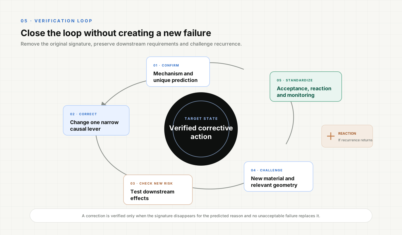
4. Verify the correction without creating a new failure
Write the confirmation experiment as a causal statement:
If mechanism X produces signature Y, changing factor Z should alter measurement M while the relevant controls remain unchanged.
Avoid changing cleaning, bake, thickness and release time together. An improved wafer would be useful but would not identify the root cause. Retain a known-good reference and define the success metric before the run. For intermittent failures, test enough features and samples to distinguish a real reduction from random absence.
Then challenge downstream compatibility. Lower stress may change resistivity or morphology. More aggressive cleaning may damage another material. A drying change may modify surface chemistry or device dynamics. Packaging changes may alter damping or heat flow.
Separate the conclusion into three levels:
- Correlation: the failure and factor changed together.
- Supported mechanism: signature, physical model and discriminating test agree.
- Verified corrective action: the change suppresses recurrence on new material without unacceptable downstream effects.
What I would do differently when troubleshooting stalls
I would stop generating more parameter changes and return to the untouched evidence. I would rebuild the signature map, verify that the measurement reproduces the apparent defect and ask which observation would most change the hypothesis ranking. I would add witness samples or simple test structures where the candidate mechanisms diverge instead of using completed devices as the only diagnostic vehicle.
The goal is not to make every investigation elaborate. It is to make each experiment answer one real question.
Before declaring a root cause
- Is the signature described without assuming the cause?
- What is the last confirmed-good inspection?
- Which mechanisms explain morphology, location and timing together?
- What unique result does each leading mechanism predict?
- Does the proposed test separate those predictions?
- Does the correction target the mechanism rather than the symptom?
- What new risk does the correction introduce?
- Has recurrence been checked on new samples and relevant geometries?
- Does the conclusion match the strength of the evidence?
Diagnosis converts defects into knowledge
MEMS failure analysis is not attaching a familiar name to an image. It is converting an observed signature into a mechanism that can be tested, corrected and monitored.
The strongest diagnosis explains morphology, location, timing, affected population and response to a controlled change. It also survives contact with the rest of the process flow: the correction does not quietly exchange one failure for another.
That is the standard worth pursuing—not a plausible story after a failed wafer, but an evidence-backed explanation that makes the next wafer more predictable.
References
- 1. J. J. Sniegowski, M. P. de Boer and N. F. Smith, “Challenges in the Packaging of MEMS,” Sandia National Laboratories, 1999.
- 2. J. M. Cassard et al., “Standard Reference Materials User’s Guide for RM 8096: MEMS 5-in-1,” NIST Special Publication 260-177, 2013.
- 3. J. Yeom, Y. Wu, J. C. Selby and M. A. Shannon, “Maximum Achievable Aspect Ratio in Deep Reactive Ion Etching of Silicon Due to Aspect Ratio Dependent Transport and the Microloading Effect,” Journal of Vacuum Science & Technology B, 23(6), 2319–2329, 2005. https://doi.org/10.1116/1.2101678
- 4. R. Legtenberg, H. A. C. Tilmans, J. Elders and M. C. Elwenspoek, “Stiction of Surface Micromachined Structures after Rinsing and Drying: Model and Investigation of Adhesion Mechanisms,” Sensors and Actuators A: Physical, 43, 230–238, 1994. https://doi.org/10.1016/0924-4247(93)00654-M
- 5. D. M. Tanner et al., “MEMS Reliability in a Vibration Environment,” Sandia National Laboratories.
Related engineering insight
Developing a Robust MEMS Process
From device requirements and controlled experiments to a stable process window.
Engineering conversation
Working through a MEMS fabrication failure?
ali.hp.shafaghi@gmail.com